PCB design
 |
The increasing complexity of electronic circuits, the miniaturization and the integration degree trends offered by electronic components market, the increasing clock speed of digital boards, CE and other normative certification requirements, and, not least, the aggressive time-to-market goals that make it necessary to rely on qualified PCB design services.
The consolidated experience in electronic design has led us over the years to face the problems of PCB development with an eye always very careful and competent to the needs of the electronic circuit, and the results, in terms of optimization and quality, have always been appreciated.
Following are the salient features of what we offer:
|
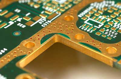
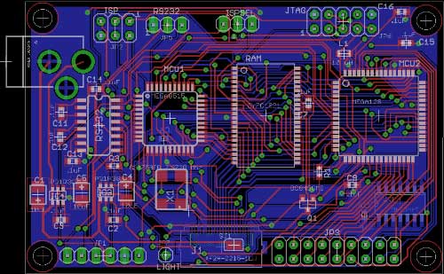
- Single-sided to multilayer PCB design, with blind / buried vias
- BGA and other high density packages management
- Routing optimization in terms of layer number and size reduction (when required)
- Careful study of component placement, in order to prioritize critical paths and functional areas of the project
- Preferential routing of critical signals with length and coupling minimization
- Effective and compliant placement and routing of noise removal components
- Striplines and connections impedance match, when required
- Power and signal tracks routing with careful to signal integrity issues and ground bounce reduction
- Tracks width and clearance adaptation to technology needing and standards compliance
- Absolute warranty of PCB design and schematic diagram match (when a netlist is provided)
- Single figure and multiplied Gerber files and production documentation (layout for pre-sized panels, files for stencils, pick and place coordinate, topological assembly, ODB ++, ...)
- Quick or standard time prototype samples can be provided
- Local and far-east located supply channels
|
 |
Do not hesitate to contact us for any evaluation or offer request.